Request Demo
Last update 08 May 2025
Photonics Research Ontario
Private Company|Canada
Private Company|Canada
Last update 08 May 2025
Overview
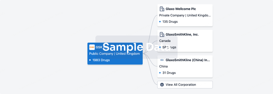
Corporation Tree
Boost your research with our corporation tree data.
login
or
Pipeline
Pipeline Snapshot as of 31 May 2025
No data posted
Login to keep update
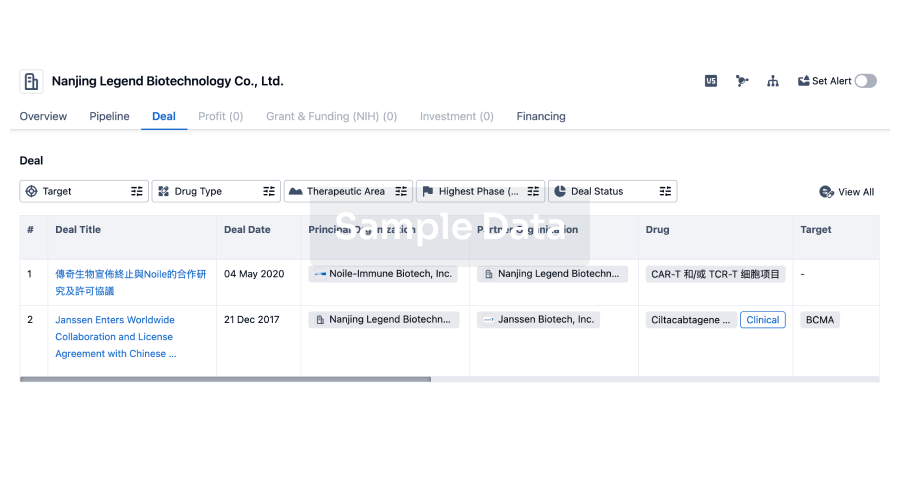
Deal
Boost your decision using our deal data.
login
or
Translational Medicine
Boost your research with our translational medicine data.
login
or

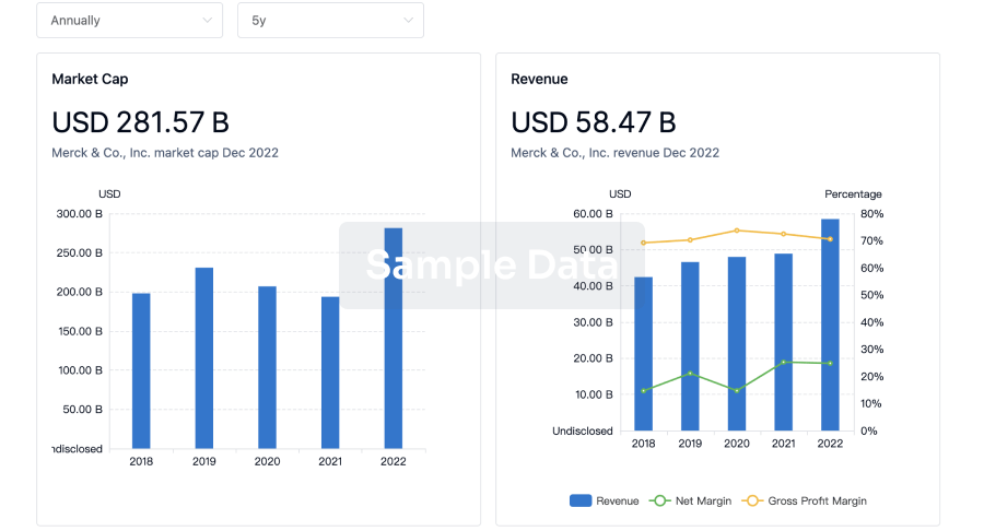
Profit
Explore the financial positions of over 360K organizations with Synapse.
login
or
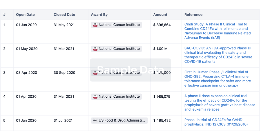
Grant & Funding(NIH)
Access more than 2 million grant and funding information to elevate your research journey.
login
or
Investment
Gain insights on the latest company investments from start-ups to established corporations.
login
or
Financing
Unearth financing trends to validate and advance investment opportunities.
login
or
AI Agents Built for Biopharma Breakthroughs
Accelerate discovery. Empower decisions. Transform outcomes.
Get started for free today!
Accelerate Strategic R&D decision making with Synapse, PatSnap’s AI-powered Connected Innovation Intelligence Platform Built for Life Sciences Professionals.
Start your data trial now!
Synapse data is also accessible to external entities via APIs or data packages. Empower better decisions with the latest in pharmaceutical intelligence.
Bio
Bio Sequences Search & Analysis
Sign up for free
Chemical
Chemical Structures Search & Analysis
Sign up for free